Scanning transmission electron microscope
Thermo-Fisher/FEI Spectra, 300 kV
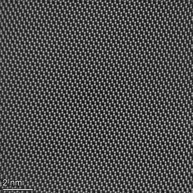
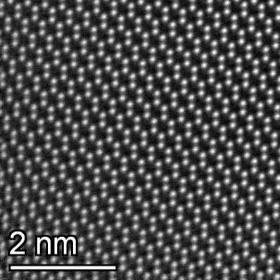
This scanning transmission electron microscope (S-TEM) provides ultra-high resolution in characterizing both structure and energy, in addition to accurate quantitative chemical analysis down to sub-angstrom level
Utilizing this new S-TEM will benefit research in nuclear materials and behaviors (diffusion along phase boundaries, for example), bringing the highest resolution imaging and spectroscopic capabilities for nuclear science post-irradiation examination in the nation
Energy spread: 0.025 eV (@ 60 kV)
Information limit: 60 pm
S-TEM resolution: 50 pm (125 pm @ 30 kV)
Technical highlights:
- Monochromated, probe- and image-corrected 30 – 300 kV HT for various applications
- Single electron sensitive S-TEM detection
- Equipped with ultra-sensitive Panther S-TEM detection system - new detector geometry offers access to advanced S-TEM imaging capability combined with the sensitivity and detectability to measure single electrons
- Eight segmented BF and ADF detectors provide the possibility of combining detector segments in arbitrary ways
- Integrated differential phase contrast (iDPC) imaging for the study of magnetic and electrical properties and for optimized Z-contrast imaging from hydrogen to uranium
- Fully automated, single-click access to the highest-resolution S-TEM (<50 pm) and energy-resolution EELS (<30 meV), drift corrected frame integration (DCFI)
- Field-free imaging in TEM Lorentz mode with 2 nm resolution for magnetic property studies
- Super-X 4 detector EDS system (≤136 eV for Mn-Kα and 10 kcps (output)), Gatan Ultrafast EELS/DualEELS.
- Electron microscope pixel array detector (EMPAD) – 4D-S-TEM
Tilt range ±40 degrees for analytical double tilt holder, ±75 degrees for tomography holder - Electron Microscope Pixel Array Detector (EMPAD) records the full diffraction pattern in one scan. Once data is acquired, BF, DF and DPC can be extracted by applying mask.
- Phase and defects can also be revealed by selecting the proper diffraction spots. EDS and 4D S-TEM mapping can be done simultaneously. Thickness can be obtained from analyzing CBED.
EDS & EELS
- Super-X is composed of 4 highly sensitive detectors with a large collection solid angle. Absence of detector window allows the detection of all elements down to boron. In addition, no stage tilting is required. Much faster than the 1-detector EDS.
- Gatan Continuum Ultrafast DualEELS can achieve the energy resolution of ≤0.2 eV (Mono ON) at 300 kV and ≤0.025 eV (UltiMono) at 30 kV. The detector can record two energy ranges at the same time. The system can support simultaneous EDS and EELS data acquisition.
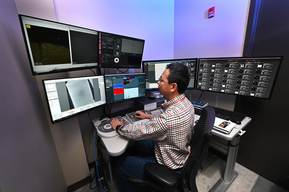
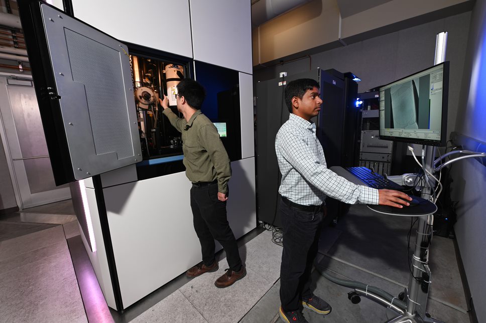
Accessing the S-TEM
The S-TEM is part of the Microscopy and Characterization Suite (MaCS), a Nuclear Science User Facilities (NSUF) laboratory accessible to students and faculty at the CAES universities and to researchers all over the world. Private industry also has access to MaCS' world-class microscopes and high-end imaging equipment. Go here for information on MaCS, including rates for utilizing the equipment, or contact us for more information.
The ease of access of CAES not only applies to students, faculty and industry; its proximity to INL's Energy Research Campus enables several INL mission areas to grow collaborative materials research programs with external partners, including the universities and industry. The S-TEM is INL's latest investment in CAES that is designed to create opportunities for collaborative materials research. CAES also is equipped with complementary materials analysis instrumentation (including a Focused Ion Bean and Local Electron Atom Probe) that will enable complete sample preparation and analysis in one location.
Advanced Manufacturing focus area
The S-TEM advances collaborative research, education and innovation at CAES in several ways, including:
- Its technological advances accelerate the timeline for nuclear innovation and modeling efforts needed to further the discovery and qualification of materials for nuclear applications, while allowing for the investigation of defects in functional energy materials found in batteries with atomic precision — a key step in improving battery performance.
- It provides a new perspective on the dynamic effects of phenomena such as irradiation damage, diffusion mechanisms and kinetics, as well as plasticity, which all must be well understood to advance materials in extreme environments such as seen in a reactor core.
- Its state-of-the-art atomic scale chemical imaging, paired with 3D tomography capability, enables new understanding of reacting interfaces of materials, providing immediate advances to collaborative CAES research currently under way in battery anodes, catalysis and corrosion.